")

In keeping with [Asianometry], nobody believed within the scanning electron microscope. Nobody, that’s, besides [Charles Oatley].The video under tells the entire story.
The Cambridge graduate constructed radios throughout World Warfare II after which joined Cambridge as a lecturer as soon as the battle was over. [Hans Busch] demonstrated utilizing magnets to maneuver electron beams, which advised the potential for making a lens, and it was an apparent thought to make a microscope that makes use of electrons.
In any case, electrons can have smaller wavelength than gentle, so a microscope utilizing electrons may — in idea — picture at a better decision. [Max Knoll] and [Ernst Ruska], in reality, developed the transmission electron microscope or TEM.
The TEM works by passing an electron beam by means of a really skinny pattern and detecting it on the opposite facet. Nonetheless, the aim was to construct an electron gadget that bounced electrons off an object — a SEM or scanning electron microscope. [Knoll] did construct a tool utilizing this precept. Nonetheless, it had a broad beam and will solely amplify 10X or so, and it didn’t scan like a contemporary scope.
A sensible SEM would watch for [Manfred Baron von Ardenne] in 1937. Working with Siemens (who, sure, owns Hackaday), he created a crude SEM. It took 20 minutes to create a picture on a bit of movie, so it wasn’t very sensible. After two years, World Warfare II broke out, and the work was misplaced.
At RCA, [Vladimir Zworykin] did some work on SEM, however deserted the poorly-working gadget as TEM units had been extra enticing. Then, within the Fifties, [Charles Oatley] determined he wished to construct an electron microscope for Cambridge.
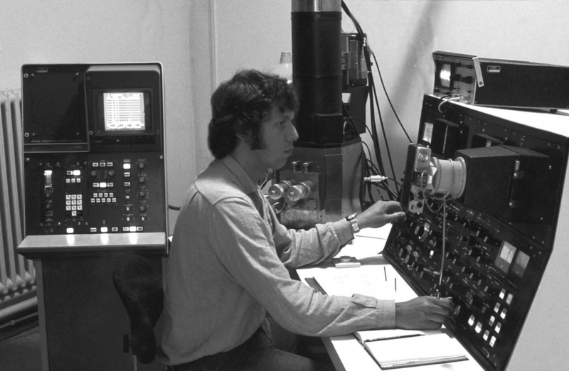
Cambridge produced a really profitable instrument that exploited secondary electrons and backscatter. They offered over 500 models. The video mentions that SEMs don’t require pattern preparation, however they actually don’t—they simply don’t require skinny slicing with a microtome. Semiconductor units are sometimes gold-coated to make the insulating floor conductive, for instance, however that’s a lot simpler to do than slicing very skinny layers.
It is a nice story of somebody with a dream to create and took a shot. Granted, the time was proper and the College was a bit simpler to please than a standard company overlord.
We’re anxious for somebody to create a DIY SEM that is buildable. For now, your finest wager is to discover a junker on the excess market and fix it up.
Picture credit score: [Hannes Grobe] CC-BY-SA 2.5